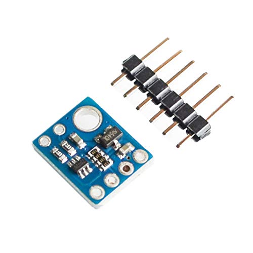
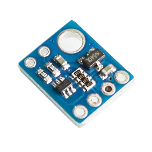
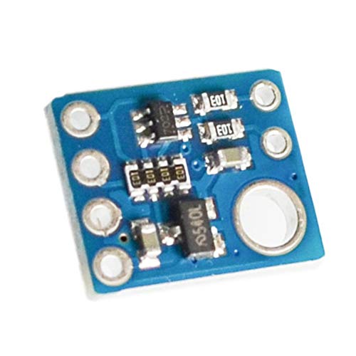
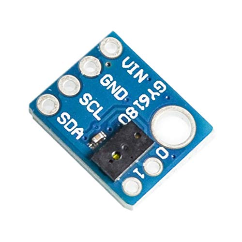
- 🌹VIN This is the main 2.7 V to 5.5 V power supply connection. The SCL and SDA level shifters pull the I²C lines high to this level.
- 🌹SDA/SDI/SDO Level-shifted I²C data line: HIGH is VIN, LOW is 0 V.
- 🌹SCL/SPC Level-shifted I²C clock line: HIGH is VIN, LOW is 0 V.
- 🌹GPIO0/CE This pin is configured as a chip enable input on power-up of the VL6180X; the board pulls it up to VDD to enable the sensor by default.
Full Reviews
-
Information
-
Twitter
-
Pinterest
-
Youtube
-
Facebook